I’m working on a custom board incorporating the CV1800B SoC as found on the Milk-V Duo and I’m studying the CVITek datasheet as well as the Milk-V Duo schematic for clues on what’s needed to hook the SoC up for proper operation. For the most part it makes sense, but one little detail is stumping me:
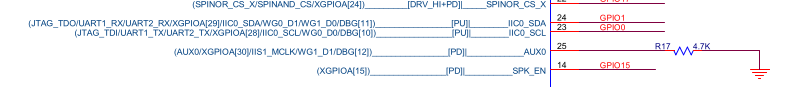
Pin 25 of the SoC is labeled “AUX0”, which appears to be an optional output from the internal clock generator and according to the 68-pin package pinout spreadsheet, on bootup it defaults to XGPIOA[30]. In the schematic it is only connected to a 4.7k resistor R17 to ground and I can’t find any detail in the datasheet for why this is needed. Does anyone know why this is? I’m guessing it’s some sort of power-up strapping but I can’t find out exactly what it does.
Doing a bit of research into this question and discovered that the Sipeed Lichee Nano also uses the SG2002 SoC with the AUX0 pin brought out to a USER button. I asked someone who has that board to capture the bootup output for both cases - with & without pressing the button and it appears that when pressed the Lichee Nano attempts to run a debugger. The code that makes the decision which path to take is in the FSBL so I’m studying that further to find out how it makes the choice.
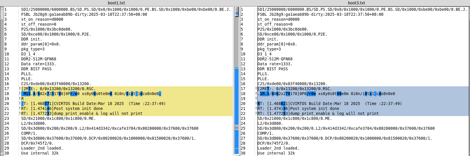
I tested it out on my Duo - soldered a jumper from the U4-25 / R17 node (AUX0 pin) to 3V3_PREI and booted up. Compared the two and didn’t see anything that appears to change except the order of some characters in the FSBL output. boot1.txt on the left is normal, boot3.txt on the right is with pullup:
Funnily enough, this topic discusses Milk-V Duo (CV1800B), SG2002 (which is on Milk-V Duo 256M board), and Duo S board (which is clear as day in your boot log above, since only SG2000 has 512M DRAM).
It confused me the first time I saw it as well. There are a lot of somewhat ambiguous things in those bootlogs. I’m especially curious about those strings of characters that change order every time it boots up - I’ve seen so many little differences in those locations even when nothing else is changing.
The reason I had this question about the AUX0 pin is that it’s the only I2S MCLK output available on the CV1800B SoC and I wanted to make sure that re-using it as an I2S signal wouldn’t interfere with whatever was going on with R17. Having confirmed that it doesn’t seem to matter I tried it out as MCLK and was successful. More detail on that here: